Electron microprobe
Albertstr. 23c (lab building), 1st floor, room 01 012, Tel.: 0761 203 6392
Contact: Dr. Dominic Wölki, Tel.: 0761 203 6388, E-mail: dominic.woelki(at)minpet.uni-freiburg.de
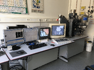
We operate Cameca SX100 electron microprobe with five WD spectrometers and an ED detector. We are expecting installation of a new field-emission electron microprobe JEOL HyperProbe JXA-iHP200F in summer 2023.
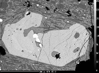
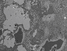
The current system allows for full spatially resolved chemical microanalysis of solid materials (2-3 um resolution). Suitable for analysis are mineral grain mounts rock sections, synthetic materials including oxides, metals or medical and organic products. The accuracy allows for measurements in tenths of one percent. The element distribution patterns can be mapped, concentration profiles can be measured for a range of geological, gemological, technical, forensic or medical applications.
 |  |  |
Detailed technical information
Cameca SX100 electron microprobe provides highly accurate, automated elemental analysis in the microresolution (um). Our instrument was installed in 1995.
Principles of microprobe analytics
• physical principle: registration of characteristic X-ray emission spectra produced by electron bombardment
• minimum spacial resolution: micrometer scale, depending on acceleration voltage and resulting penetration depth of the electron beam
• detection limits: element and matrix dependent, some tens to some hundreds ppm
• accuracy: element and matrix dependent, 1 - 3 relative percent (for Z < 11 much worse)
• reproducability: concentration and measuring time dependent: ~ 1 relative percent
• analysis time: concentration and necessary accuracy dependent: some ten to some hundred seconds per element (WDS)
Sample requirements:
• For quantitative work all samples must be flat and mounted perpendicular to the electron beam.
• Materials must be stable under electron bombardment and vacuum conditions.
• Standard geological applications require uncovered thin sections with 0.5 µm diamond powder polishing.
• Samples have to be electronically conductive or coated with some conductive material (typically carbon).
• In general samples have to be regarded as being homogeneous on the micrometer scale. Special correction procedures are needed for thin films and single particles.
Features of our SX100:
• 50 kV electron gun, W-filament
• Spectrometers:
Five vertical wavelength-dispersive spectrometers (PC0 - PC3 = synthetic multilayers):
| No. | Crystals | Special features |
| 1 | TAP, PCO | -- |
| 2 | LIF, PET | "high pressure" proportional counte |
| 3 | LIF, PET | "high pressure" proportional counte |
| 4 | TAP, PET, PC1, PC3 | -- |
| 5 | TAP, PET, LIF, PC2 | extended 2theta range, allowing O Ka to be measured on the TAP xtal |
Element range covered (theoretically, element specific inconveniences occur):
| Crystal | Formula | 2d [Å] | K shell | L shell |
| PC3 | Mo/B4C Multilayer | 200 | Be-B | |
| PC2 | Ni/C Multilayer | 95 | B-O | |
| PC1 | W/Si Multilayer | 60 | C-F | |
| PC0 | W/Si Multilayer | 45 | O-F | |
| TAP | C8H5O4Tl | 27.745 | F-P | Mn-Nb |
| PET | C5H12O4 | 8.742 | Si-Mn | Sr-Tb |
| LIF | LiF | 4.027 | Sc-Rb | Te-U |
The system is integrated with a Link (Oxford) nitrogen cooled ED-system, specified resolution 138 eV, standard Be-window, element range Na-U.
• Specimen stage: The minimum step size is 0.5 µm. Accommodation of a wide range of samples sizes, including 40mm round, 48*28mm, 30*30mm, but the standard size being either 1 inch (25.4mm) round or 28 x 48 mm sized thin sections; maximum specimen size 75*50*25 mm. A maximum of 6 samples/standards of the standard size (1in) can be loaded at the same time.
• Optical microscope: reflected and transmitted light optics and polariser. The magnification is fixed to 400. An attached color CCD camera provides an image on the computer screen.
• Vacuum system: Cameca standard vacuum system.
• Anticontamination: Equipment comprising a liquid nitrogen cold finger near the point of impact of the electron beam, and an oxygen jet to burn off carbon contamination.
A variety of standard materials that cover most geological and materials science applications is available. The original file format of analysis data is ASCII, which is easily converted to Excel 5. Possible image formats are "Cameca" (ASCII), Sun Raster or TIFF. Only the Cameca format contains information about analysis conditions.